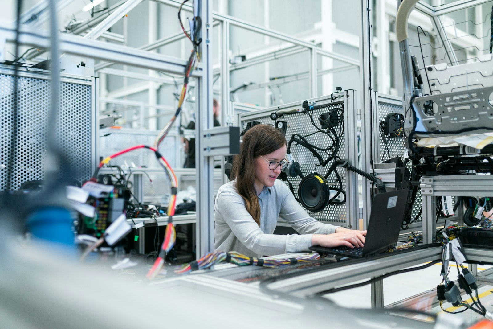
Cleanroom Complex (Class 1000 + Class 100)
A process-development and prototype facility — not a high-volume CMOS fab.
Capabilities
Photolithography and deposition systems · Microfabrication for sensors, MEMS and photonics · Wafer-level characterisation tools · Materials analysis — SEM, AFM, XRD via shared-facility partnerships.
Phased Development
Phase 0 — validate demand: user consortium, priority device families, letters of intent, process/EHS/utility DPRs. Phase 1 — commission core prototyping: cleanroom shell, certified procedures, baseline lithography, thin-film, wet-process, etch/thermal and metrology. Phase 2 — expand by utilisation: specialised processes, packaging interfaces and advanced materials/device modules.
Who Benefits
MEMS and sensor startups avoid the capital cost of a private cleanroom · Photonics, microfluidics and device researchers validate processes locally · Corporate R&D teams run pilot runs and process development · A trained cleanroom workforce is created for Kerala's emerging device ecosystem.
Design-to-Device Pathway
Direct linkage from K-SDC designs to cleanroom prototyping, on to IIoT integration and Maker Village 2.0 productization — reducing coordination risk and improving the probability that a design becomes a marketable product.
Explore related
Semicon Keralam Headquarters
Central coordinating authority for all State-level semiconductor initiatives
Kerala Semiconductor Design Centre (K-SDC)
Flagship end-to-end chip design, verification and prototyping facility
Kerala Semiconductor Cloud (K-SC)
Statewide virtual semiconductor design platform